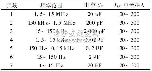
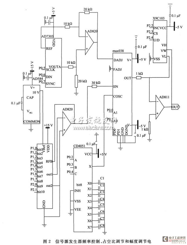
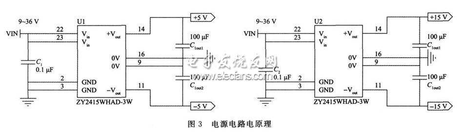
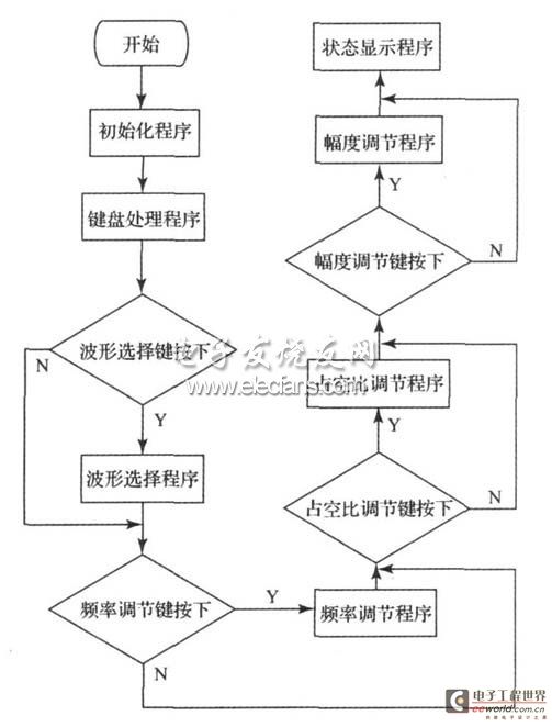
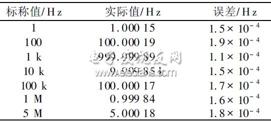
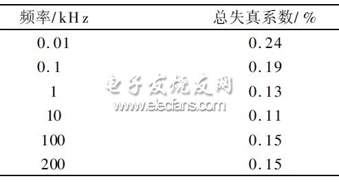
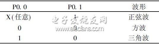
introduction The signal source generation circuit can be made up of an RC oscillating circuit, an LC oscillating circuit, and an oscillating circuit composed of 555 timers, and more is generated by a special function signal generator IC, but they have less functions and are not accurate. The upper frequency limit is only 300 kHz, and the higher frequency signal cannot be generated. In addition, the adjustment method is not flexible enough. The frequency and duty ratio cannot be adjusted independently, and the two affect each other. There are also signal generators that use a dedicated DDS chip, but the circuit structure is complicated and the cost is high. The signal source specifically designed for very low frequencies has a narrow design frequency range and a small application range. To this end, this paper studies and designs a signal source generator based on single-chip microcomputer C8051F130 and MAX038, which can generate triangular wave, sine wave and square wave in 15 MHz. It has high precision and small distortion, which can effectively compensate for the above design. , to meet the requirements of most of the test source. 1 Overall design of the signal source generator The signal source generator mainly uses the single chip C8051F130 as the control core. Through the control of Maxim's waveform generator chip MAX038 and its external circuit, it realizes the output of different amplitudes and frequencies and different types of signals. The C8051F130 is launched by Silicon Laboratories. An integrated mixed-signal system-on-chip with 8051 core and instruction set compatibility. It can execute instructions up to 100 MIPS, and has 8448 (8K+ 256) bytes of on-chip RAM and 128 Kbytes of flash memory. With up to 64 input and output ports, it can fully meet the control requirements of this design. The MAX038 is a waveform generator that requires only a few external components to generate accurate sine, triangle and square waves. The output frequency and duty cycle can pass through the periphery. The current, voltage and resistance of the circuit are adjusted. The whole signal source generator is composed of a frequency control part, a waveform selection part, a duty ratio adjustment part, a keyboard input control part, a signal state display part, a power supply part, etc. The circuit block diagram is shown in FIG. Figure 1 signal source generator 2 signal source generator hardware circuit design 2. 1 Waveform selection section Use the I/O port P0. 0 and P0. 1 on the C8051F130 to connect the A0 and A1 pins on the MAX038. Set the input to generate sine, square and triangle waves. The relationship between the pin level and the waveform is shown in the table. 1 is shown. Table 1 A0 and A1 pin level corresponding waveform relationship The switchover time is less than 0.3 us, regardless of the phase of the output signal. 2. 2 frequency control part The frequency of the MAX038 output signal is determined by the current IIN injected into pin IIN, the capacitor CF terminated at the COSC pin, and the voltage V FADJ at pin FADJ. When VFADJ = 0 V, the basic output frequency Fo is given by: Where: IIN is the current flowing into the IIN pin (10 A to 400 A for best performance), CF is the capacitance connecting the COSC pin and ground (selected in 20 pF~ 100 F), if VFADJ is already For example, any output frequency Fx = Fo [ 1- (0. 2915 VFADJ ) ], in this design, a different voltage is output through the 10-bit D/A converter A D7533, and a 30 kΩ resistor is connected to the MAX038 IIN tube. The current of the pin and the C8051F130 control CD4051 select different CF to determine the output frequency value of the signal. The frequency of the whole output signal is divided into 7 frequency bands. The correspondence between the frequency band division and the CF value and the inflow IIN current value are shown in Table 2. Table 2 Correspondence between frequency band division and CF value and inflow IIN current value 2. 3 duty cycle adjustment section The voltage on the DADJ pin controls the duty cycle of the output waveform. When VDADJ = 0, the duty cycle is 50%. When the voltage is from + 2. 3 V to - 2. 3 V, the output duty cycle is 15%. ~ 85% change, voltage change 1 V can change the duty cycle by 15%, the duty cycle adjustment part selects the AD7303 8-bit D/A converter with serial input and dual voltage output, and controls the AD7303 output through C8051F130 - 2. 3 ~ + 2. 3 V, Connect to the DADJ pin to adjust the duty cycle. 2. 4 amplitude adjustment section After frequency control and duty cycle adjustment, the MAX038 output can output a waveform of amplitude 2 V (VPP), which is -1~ + 1 V to ground symmetry, and the output impedance is less than 0. 1 Ω provides ±20 mA drive current directly to a 50 pF capacitive load. In order to meet the requirements of the actual use of the signal source, the amplitude adjustment circuit is also required to adjust the output signal amplitude and increase the signal driving capability. The amplitude adjustment circuit is composed of an inverse proportional operation circuit composed of a wideband high-speed current feedback operational amplifier AD811, wherein the feedback resistance is composed of The MCU C8051F130 controls the X9C103 digital potentiometer. The output signal can vary from 200 mV to 20 V (VPP) with the gain of the op amp. The step size is 200 mV (VPP). Figure 2 shows the electrical schematic of the signal source generator frequency control section, the duty cycle adjustment section, and the amplitude adjustment section. 2. 5 power section The power circuit part mainly supplies the voltage required for the operation of each chip to other circuits, and needs + 15 V, - 15 V, + 5 V, - 5 V. In order to reduce the influence of power supply interference on each part of the circuit, especially for D/ A converter converter conversion accuracy, using the wide-voltage input isolation regulator positive and negative dual output isolation power chip ZY _WHAD- 3W series produced by Guangzhou Zhou Ligong, which has high conversion efficiency, good high and low temperature characteristics, high voltage accuracy, etc. In addition, the + 10 V reference voltage required for the A D7533 operation is provided by the AD584 (see Figure 2). The power circuit schematic is shown in Figure 3. 2. 6 keyboard input and signal status display The part of the circuit uses the liquid crystal display module SG19264 and the key switch to realize the frequency, amplitude, duty cycle adjustment and signal status output display of the signal source generator. The I/O port of the C8051F130 is used to connect the 4 4 ​​keyboard matrix and the SG19264 data port and control port. According to the button status, the output signal type, frequency, amplitude, duty cycle and other status information are displayed on the liquid crystal module. 3 software design The signal generator software is designed with modular programming structure, which is divided into initialization program, keyboard processing program, waveform selection program, frequency adjustment program, duty cycle adjustment program, amplitude adjustment program, signal status display program, and signal generator power-on initialization. The program generates a square wave with a frequency of 1 kHz, an amplitude of 2 V (VPP), and a duty cycle of 50%. After the initialization, the response is pressed by the button, and the corresponding signal state adjustment program is finally displayed on the liquid crystal through the signal state display program. The program flow chart is shown in Figure 4. Figure 4 program flow 4 Conclusion In order to verify the performance of the designed signal source generator, after the hardware and software design described above, the actual parameters of the output signal parameters were tested. The Agilent 53132A and National VP7720A were used to output the frequency accuracy and total distortion of the main parameters. The test data for the coefficients are shown in Tables 3 and 4. Table 3 Output frequency Table 4 sine wave distortion coefficient It can be seen from Table 3 and Table 4 that the signal generator of this design can achieve an output waveform distortion of less than 0.3%, and the output frequency accuracy is better than 2 × 10 - 4 , which is superior in the same design. It has been verified by experiments that the designed signal generator can output a frequency less than 15 MHz, the amplitude is 200 mV~ 20 V (VPP) continuously adjustable, and the duty cycle is 15%~855% square wave, sine wave, triangle wave, with periphery The circuit has the advantages of simple circuit, small volume, high precision and small distortion of output waveform. This signal generator has been widely used in electrical electrical testing work in our hospital.
Quality series light duty industrial caster
Popular in each market, most welcomed type
Ningbo Mywin Caster Co., Ltd. , https://www.mywin-caster.com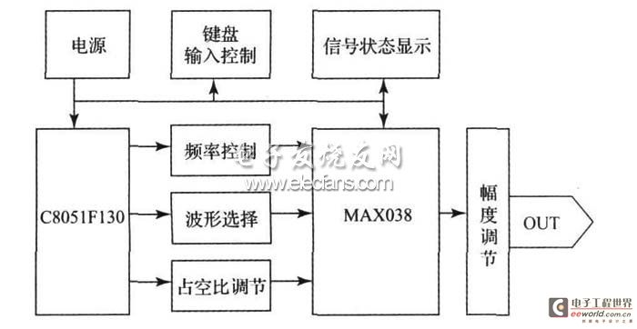
![]()